PCIe memory development card
December 5th, 2017
Our client, the industry leader in memory devices, required a PCIe x16 based development board for their next generation of memory.
Challenges
- Define a stack-up that would allow sufficient pin escape of a 1932 pin FPGA whilst maintaining trace impedance and delivering multiple power rails in to the FPGA. Individual rails delivering up to 32A in to the FPGA
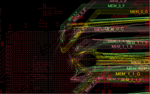
- 16 different memory banks connected to the FPGA, some pin swapping was available at the FPGA, so significant routing planning was required
Solution
- Calculate number of signal layers required based on quantity of nets from FPGA, using number of nets per layer based on estimated track and gap
- Calculate number of power layers bases on the current capacity per layer and an estimate of which power signals will be on which layers
- Using the FlowPlan Cadence tool to allow the grouping of nets within each bus/net group, then place each bus as a wide trace on the selected layer
Outcome and Technologies
- 16 Layer conventional construction PCB with mixed copper weights
- Power planning ensured that no impedance controlled nets crossed power plane splits
- Power distribution was sufficient with adequate current delivery and acceptable voltage drop as simulated by power integrity tools